- 您现在的位置:买卖IC网 > Sheet目录3875 > PIC18F44K20-I/MV (Microchip Technology)MCU 16KB FLASH 768B RAM 40-UQFN
2007 Microchip Technology Inc.
Preliminary
DS70165E-page 159
dsPIC33F
10.0
I/O PORTS
All of the device pins (except VDD, VSS, MCLR and
OSC1/CLKIN) are shared between the peripherals and
the parallel I/O ports. All I/O input ports feature Schmitt
Trigger inputs for improved noise immunity.
10.1
Parallel I/O (PIO) Ports
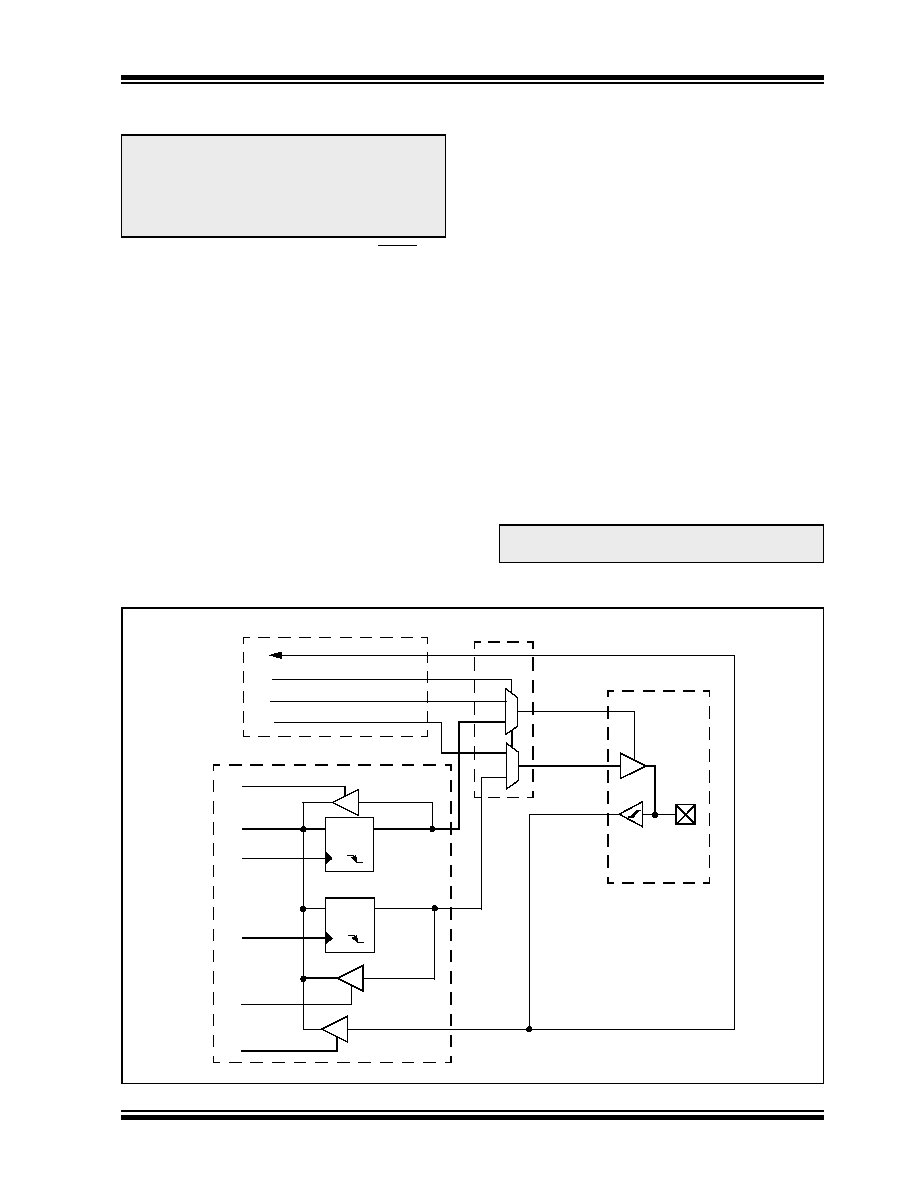
A parallel I/O port that shares a pin with a peripheral is,
in general, subservient to the peripheral. The periph-
eral’s output buffer data and control signals are
provided to a pair of multiplexers. The multiplexers
select whether the peripheral or the associated port
has ownership of the output data and control signals of
the I/O pin. The logic also prevents “loop through”, in
which a port’s digital output can drive the input of a
peripheral that shares the same pin. Figure 10-1 shows
how ports are shared with other peripherals and the
associated I/O pin to which they are connected.
When a peripheral is enabled and actively driving an
associated pin, the use of the pin as a general purpose
output pin is disabled. The I/O pin may be read, but the
output driver for the parallel port bit will be disabled. If
a peripheral is enabled, but the peripheral is not
actively driving a pin, that pin may be driven by a port.
All port pins have three registers directly associated
with their operation as digital I/O. The data direction
register (TRISx) determines whether the pin is an input
or an output. If the data direction bit is a ‘1’, then the pin
is an input. All port pins are defined as inputs after a
Reset. Reads from the latch (LATx), read the latch.
Writes to the latch, write the latch. Reads from the port
(PORTx), read the port pins, while writes to the port
pins, write the latch.
Any bit and its associated data and control registers
that are not valid for a particular device will be
disabled. That means the corresponding LATx and
TRISx registers and the port pins will read as zeros.
When a pin is shared with another peripheral or func-
tion that is defined as an input only, it is nevertheless
regarded as a dedicated port because there is no
other competing source of outputs. An example is the
INT4 pin.
FIGURE 10-1:
BLOCK DIAGRAM OF A TYPICAL SHARED PORT STRUCTURE
Note:
This data sheet summarizes the features
of this group of dsPIC33F devices. It is not
intended to be a comprehensive reference
source. To complement the information in
this data sheet, refer to the “dsPIC30F
Family Reference Manual” (DS70046).
Note:
The voltage on a digital input pin can be
between -0.3V to 5.6V.
Q
D
CK
WR LAT +
TRIS Latch
I/O Pin
WR PORT
Data Bus
Q
D
CK
Data Latch
Read Port
Read TRIS
1
0
1
0
WR TRIS
Peripheral Output Data
Output Enable
Peripheral Input Data
I/O
Peripheral Module
Peripheral Output Enable
PIO Module
Output Multiplexers
Output Data
Input Data
Peripheral Module Enable
Read LAT
发布紧急采购,3分钟左右您将得到回复。
相关PDF资料
PIC16C622A-20/P
IC MCU OTP 2KX14 COMP 18DIP
PIC16LF727-I/MV
MCU PIC 14KB FLASH XLP 40-UQFN
PIC12C672-10/P
IC MCU OTP 2KX14 A/D 8DIP
PIC18F44J10-I/ML
IC PIC MCU FLASH 8KX16 44QFN
PIC16F628A-I/P
IC MCU FLASH 2KX14 EEPROM 18DIP
PIC18F24K22-I/SO
IC PIC MCU 16KB FLASH 28SOIC
PIC18F23K22-I/SP
IC PIC MCU 8KB FLASH 28SPDIP
PIC18LF23K22-I/SP
IC PIC MCU 8KB FLASH 28SPDIP
相关代理商/技术参数
PIC18F44K20-I/P
功能描述:8位微控制器 -MCU 16KB Flash 768B RAM 36 I/O 8B RoHS:否 制造商:Silicon Labs 核心:8051 处理器系列:C8051F39x 数据总线宽度:8 bit 最大时钟频率:50 MHz 程序存储器大小:16 KB 数据 RAM 大小:1 KB 片上 ADC:Yes 工作电源电压:1.8 V to 3.6 V 工作温度范围:- 40 C to + 105 C 封装 / 箱体:QFN-20 安装风格:SMD/SMT
PIC18F44K20-I/PT
功能描述:8位微控制器 -MCU 16KB Flash 768B RAM 36 I/O 8B RoHS:否 制造商:Silicon Labs 核心:8051 处理器系列:C8051F39x 数据总线宽度:8 bit 最大时钟频率:50 MHz 程序存储器大小:16 KB 数据 RAM 大小:1 KB 片上 ADC:Yes 工作电源电压:1.8 V to 3.6 V 工作温度范围:- 40 C to + 105 C 封装 / 箱体:QFN-20 安装风格:SMD/SMT
PIC18F44K20T-I/ML
功能描述:8位微控制器 -MCU 16KB Flash 768B RAM 36 I/O 8B RoHS:否 制造商:Silicon Labs 核心:8051 处理器系列:C8051F39x 数据总线宽度:8 bit 最大时钟频率:50 MHz 程序存储器大小:16 KB 数据 RAM 大小:1 KB 片上 ADC:Yes 工作电源电压:1.8 V to 3.6 V 工作温度范围:- 40 C to + 105 C 封装 / 箱体:QFN-20 安装风格:SMD/SMT
PIC18F44K20T-I/MV
功能描述:8位微控制器 -MCU 16KB FL 768b-RAM 8b Familynanowatt XLP
RoHS:否 制造商:Silicon Labs 核心:8051 处理器系列:C8051F39x 数据总线宽度:8 bit 最大时钟频率:50 MHz 程序存储器大小:16 KB 数据 RAM 大小:1 KB 片上 ADC:Yes 工作电源电压:1.8 V to 3.6 V 工作温度范围:- 40 C to + 105 C 封装 / 箱体:QFN-20 安装风格:SMD/SMT
PIC18F44K20T-I/PT
功能描述:8位微控制器 -MCU 16KB Flash 768B RAM 36 I/O 8B RoHS:否 制造商:Silicon Labs 核心:8051 处理器系列:C8051F39x 数据总线宽度:8 bit 最大时钟频率:50 MHz 程序存储器大小:16 KB 数据 RAM 大小:1 KB 片上 ADC:Yes 工作电源电压:1.8 V to 3.6 V 工作温度范围:- 40 C to + 105 C 封装 / 箱体:QFN-20 安装风格:SMD/SMT
PIC18F44K22-E/ML
功能描述:8位微控制器 -MCU 16KB Flash 768B RAM 8b FamilynanoWat XLP RoHS:否 制造商:Silicon Labs 核心:8051 处理器系列:C8051F39x 数据总线宽度:8 bit 最大时钟频率:50 MHz 程序存储器大小:16 KB 数据 RAM 大小:1 KB 片上 ADC:Yes 工作电源电压:1.8 V to 3.6 V 工作温度范围:- 40 C to + 105 C 封装 / 箱体:QFN-20 安装风格:SMD/SMT
PIC18F44K22-E/MV
功能描述:8位微控制器 -MCU 16KB FL 768b RAM8bit familynanoWatt XLP RoHS:否 制造商:Silicon Labs 核心:8051 处理器系列:C8051F39x 数据总线宽度:8 bit 最大时钟频率:50 MHz 程序存储器大小:16 KB 数据 RAM 大小:1 KB 片上 ADC:Yes 工作电源电压:1.8 V to 3.6 V 工作温度范围:- 40 C to + 105 C 封装 / 箱体:QFN-20 安装风格:SMD/SMT
PIC18F44K22-E/P
功能描述:8位微控制器 -MCU 16KB Flash 768B RAM 8b FamilynanoWat XLP RoHS:否 制造商:Silicon Labs 核心:8051 处理器系列:C8051F39x 数据总线宽度:8 bit 最大时钟频率:50 MHz 程序存储器大小:16 KB 数据 RAM 大小:1 KB 片上 ADC:Yes 工作电源电压:1.8 V to 3.6 V 工作温度范围:- 40 C to + 105 C 封装 / 箱体:QFN-20 安装风格:SMD/SMT